Mechanics and Construction of the LED Microscope Bulb
A LED is basically a diode, in this case a Light Emitting Diode. Diodes are made of two very thin layers of material, one layer will have an excess of electrons, while the other has a deficit of electrons.
If a current is connected to the both sides of a diode, then the difference in the both layers causes the electrons to move from one layer to the other and so current is flowing.
The fun thing is that when we reverse the current leads (+ and-), the current is blocked (one layer has no electrons enough to conduct).
The diode can be used as an electronic “one direction street”. In the past hundred years the diode has brought us a lot of technical progress.
Experiments in earlier days on its properties led to the discovery that if the diode was made out of other material layers, the diode started to radiate some visible red light. Now new materials and new techniques are used to expand this invention.
One of the latest ultramodern ways of producing LEDs for home and street lighting, has been made public by Osram. Osram shows us a way of production that looks somewhat like pasting a sandwich........... but then extremely high tech.
Mechanics and Procedure
When a material like that of metal is heated enough it starts to evaporate. When this vapour comes in contact with its surroundings, the vapour will stick to it like soot from a candle.
Of course the scientists are advanced in their thinking and use specially selected materials to evaporate in a vacuum. These materials settle on a specific (disc shape) carrier material in such a way that the result is a fine evenly spread layer of a certain thickness (however, thick is actually very thin, like maybe less then 2 micron where 1 micron = 1 thousandth of a mm).
As I previously mentioned to describe this process, it is much like “pasting a sandwich”. First, we have our disc shape “sandwich” with the first layer “butter” on it.
In the same way a second or a third layer can be put on top of the first one. The result is a silver shiny layer with a conducting layer on top.
Now our "sandwich" is ready, but scientists have discovered how to emit more light from the diode, hence the mirror layer.
They peel the “sandwich” from the back of our “buttering”, and put the buttering upside down on a new, easy to process hard carrier that can conduct current.
Now the conducting and mirror layer are in the back, so when the diode layers, which are very thin and somewhat transparent, start to emit light, it will also be reflected from behind.
Efficiency level is much higher now.

LED Microscope Bulb Construction
This new hard carrier (with a diameter of about 15 cm) is cut into tiny squares, each of those squares is a LED chip..... about 17.000 in one go (New machines are made now to handle carriers of 20 cm diameter, this will produce well over 30.000 chips in one go)
Now one more thing is needed to make a useful LED from the chip.
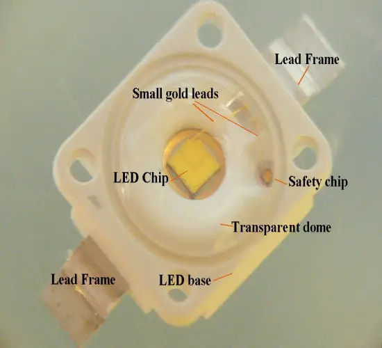
While cutting the disc, they do not cut the carrier completely, but leave the chips somewhat connected. Such a carrier is fed into a machine that picks one square at a time, and cements it on a lead-frame - an endless metal connector strip which will finally be the “wires” of the separate LEDs as we know it.
A very special soldering machine “bonds” one, two or more extremely thin gold wires from the chip to the lead-frame, so the electrical connection is made to the chip.
Then a housing and a transparent cover is put over the construction, and the lead-frame is cut, so we end up with a load of single, working LEDs.
In the image: Through the transparent cover of the LED you can actually see the (yellow) chip, cemented on the leads, and the tiny connecting wires.
Return to Dimming the LED Microscope Bulb
Return to MicroscopeMaster Home
Find out how to advertise on MicroscopeMaster!


MicroscopeMaster.com is a participant in the Amazon Services LLC Associates Program, an affiliate advertising program designed to provide a means to earn fees by linking to Amazon.com and affiliated sites.
Recent Articles
-
Deltaproteobacteria - Examples and Characteristics
Nov 01, 22 04:44 PM
 Deltaproteobacteria is a large group (Class) of Gram-negative bacteria within the Phylum Proteobacteria. It consists of ecologically and metabolically diverse members. Read more here.
 -
Chemoorganotrophs - Definition, and Examples
Oct 26, 22 05:01 PM
 Chemoorganotrophs also known as organotrophs, include organisms that obtain their energy from organic chemicals like glucose. This process is known as chemoorganotrophy. Read more here.
 -
Betaproteobacteria – Examples, Characteristics and Function
Oct 25, 22 03:44 PM
 Betaproteobacteria is a heterogeneous group in the phylum Proteobacteria whose members can be found in a range of habitats from wastewater and hot springs to the Antarctic. Read more here.