Nanonics Optometronic 4000SPM
Technology at its Finest
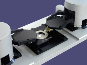
The Nanonics Optometronic 4000 is a powerful device engineered to observe and manipulate on the nano-scale. A Near-field Scanning Optical Microscope (NSOM), the Optometronic combines Nanonics’ pioneering multi-probe and atomic force capabilities with new nanomanipulation technology.
This enables advanced studies in the areas of photonics and of plasmonics, which can lead to potential advancements in fields such as health, energy, technology, environment and communications.
Nanonics

Founded in 1997, Nanonics Imaging, Ltd. is the leader in Scanning Probe Microscopes (SPM), Atomic Force Microscopes (AFM) and Near-field Scanning Optical Microscopes (NSOM/SNOM).
Located in Israel, Nanonics developers work alongside Professor Aaron Lewis – one of the architects of SPM technology.
Aside from their multiple patents, which include a range of probes and 3D Flat Scanning Technology, Nanonics has been the recipient of many awards, including honors in the R&D 100 -- recognition for the Optometronic 4000 in 2007. The company not only sets itself apart with innovation, but with a dedicated, knowledgeable team, which provides installation and customer service for the life of a system.
Providing further credence to the company’s reputation are the many published researchers around the world whose studies are made possible by technologies found in the Nanonics Optometronic 4000 and other microscopic systems – most recently, gateways into the analysis of SPPs.
Nanonics and Scanning Probe Microscopy
Nanonics is the global leader in Scanning Probe technology. Revolutionary concepts are not limited to invention, but the ingenuity to combine multiple systems together – as in the Nanonics Optometronic 4000.
Scanning Probe Microscopy (SPM) refers to systems that utilize the tip of a cantilever to observe or manipulate a specimen. SPM technology removes the former limitations of observations dependent on the wavelengths of photons or electrons and makes 3D surface imaging a reality.
The properties of probes are a determinate factor in observations; tips of cantilevers can vary in:
- Size – up to 10s of nm
- Material – glass or metal
- Coating – Au (Gold), Ti (Titanium), Cr (Chromium) or Ag (Silver)
- Mode
The primary methods of operation are contact, non-contact and dynamic or “tapping” mode, the latter two employ oscillating stiff cantilevers. Magnetic and electrically charged tips as well as oscillating the sample under a still probe provide additional topographical data.
With near-field and atomic force capabilities, the Nanonics Optometronic 4000 is the device for nano-photonic and plasmonic research. The full implication of the study of surface plasmon polaritons (SPPs) is fueled with possibilities for advancements in energy, medicine, electronic devices and transmitters.
From Light to Electron
Understanding the significance of SPM technology requires a brief grounding in the former limitations of microscopy.
Comprised of a lens, stage and illumination source, optical microscopes were limited to the diffraction of light; specifically and based on Ernst Abbe’s formula, the greatest possible resolution using an incidental light source in the wide-field was calculated at 200 nm.
Objectives and techniques such as dark-field, polarization, epi-fluorescence and phase contrast increase the possibilities of what can be seen; however, traditional optical microscopy remains restricted by the wavelength of light.
Attributed to the Nobel Prize work of Ernst Ruska and considered one of the most influential innovations of the 20th century, the electron microscope (EM) was far more powerful that its optical predecessors.
Ruska believed a microscope that concentrated on electrons, rather than photons, would yield access to more finite information given the shorter wavelength.
EMs such as the transmission electron microscope (TEM), scanning electron microscope (SEM) and scanning tunneling microscope (STM) enabled nanoscale observations, from 1 to 100 nm.
Despite their many advantages, EMs are large, cumbersome to maintain and sensitive to extrinsic effects on the magnetic field.
The STM was the first scanning probe system; like other EMs, it requires the use of quantum tunneling to capture excited-electrons escaping a sample to provide topographical, morphographical, compositional and crystallographic data.
The STM, however, is limited to observations of samples with conducting or semi-conducting surfaces.
Atomic Force Microscopy
The first Atomic Force Microscopes (AFM), invented in the mid-1980s by Nobel Prize Awarded Gerd Bennig and Calvin Quate, was used in conjunction with an STM.
AFMs use probes to gather surface data, but do not have the limits of STM; specifically, AFMs can provide imaging of almost any type of surface – including non-conducting surfaces such as ceramics, glass, polymers and even certain biological samples as well as multiple environments such as air, liquid and vacuum.
Imaging comes from the measured force between the probe and specimen, calculated by the deflection, distance and stiffness of the cantilever. In addition, AFMs have the capacity for micromanipulation of individual atoms and molecules.
The “stage” of an AFM consists of piezocrystals or piezoelectric elements – conduits of sort that expand and contract; electric polarization can occur from mechanical stressors or mechanical movements can result from applied electrical voltage.
The Nanonics Optometronic 4000 contains 3D flat scanning – a system that contains four piezos in a cylindrical tube and allows researchers the ability to operate each piezo stage independently.
The patented Piezo stage features are uniquely suited for plasmonics and photonics research:
- A large z-axis provides a bridge to use with confocal imaging
- Accurate tip-sample alignment
- Thin plate – 7mm
- Accommodates varying sizes and shapes, including large or atypical samples
- Control over inertial motion and offsets
- X, Y, Z motorized stages
In addition, Nanonics Optometronic 4000 uses online AFM/Raman Spectroscopy (SERS) and Tip Enhanced Raman Spectroscopy (TERS), Alternating Current (AC) mode (tapping) as well as all modes of AFM probe operation.
It serves as a compliment to NSOM technology – making this system one of the most powerful and diversified available to date.
Near-Field Scanning Optical Microscopy - A Brief History
Despite certain attempts to increase the diffraction of light via sub-wavelength imaging such as apodization, liquid immersion, confocal techniques and lithography, the limits defined in Abbe’s formula were never overcome until the invention of Near-Field scanning optical microscopy (NSOM) – resolution estimated at 50-100nm.
Near-field technology, such as that possible with the Nanonics Optometronic 4000, brought photons back into microscopy.
Although a handful of scientists are ascribed with the notion, E. Ash and G. Nicholls were the first to access the near-field using microwave technology in 1972.
In the 1980s, researchers at IBM in Zurich successfully developed a scanning near-field microscope (SNOM), while scientists at New York’s Cornell University also had similar success. However, the most significant developments – the feedback system and implementation of an optical fiber probe – are credited to the work of Eric Betzig. Since the early 1990s, researchers have worked to expand the capabilities of NSOM technology and its applications.
Professor Aaron Lewis, founder of Nanonics, first began considering solutions to the near-field in 1979. A Physics professor at Cornell, he felt “stymied” in his own research by the limits of “lenses, prisms and mirrors;” although it would be decades before his idea would come to fruition, by creating an extremely small hole in a metal film to illuminate the near-field – a section of the wavelength of light previously inaccessible.
The high-resolution images obtained by essentially removing the accepted limitations of observations contingent on the diffraction of incidental light is a reality because of the ground-breaking nature of the work of scientists such as Prof. Lewis and his Nanonics colleagues.
However, this achievement is grossly understated when taking into consideration that many of the nano-tools required to create the minute illumination aperture had not been or were in the process of being fabricated during the development of the NSOM system.
Advancements in AFM technologies were most valuable in achieving near-field observation.
NSOM
NSOM technology, like AFM, uses probes to analyze a sample; rather than measure force, imaging results from capturing light before it propagates or diffracts into the far-field. This is referred to as non-diffraction-limited high-resolution optical imaging and is captured within 10s of nanometers from the sample surface.
Nanoparticles, compared to observing larger samples, have a larger degree of surface area exposure and surface activity. Because of the variety of cantilevers and tips used in NSOM technology, researchers are able to obtain a comprehensive picture by studying the surface excitability in relation to light, material (metal, glass), distance and method.
In the case of SPPs, researchers were unable to confirm properties or begin to realize the full photonic potential because electromagnetic excitation can only be measured within nano-meters of the surface.
The combination of probes and the light that comes through the small aperture – smaller than the wavelength of light – allows researchers to observe interference that occurs in the near-field and apply this knowledge to the development of nano-photonic and optoelectronic applications.
Unlike traditional light microscopy, where the distance between the specimen and light source is greater than the wavelength of light, near-field or evanescent observations can only occur within a distance less than the wavelength of light; in addition, the ratio of surface size illuminated is much smaller in near-field when compared to far-field.
Operators of NSOM devices rely on scanning probe and feedback systems to avoid making contact with specimen. Nanonics Optometronic 4000 employs “tuning fork” feedback systems that allows for online feedback of multiple probes simultaneously.
Used both in AFM and NSOM, the tuning fork system decreases the chance of artifacts as there is no risk of unwanted interference, such as that which could come from laser feedback.
Nanonics not only provides an efficient means to control multiple probes, their system is easy for users to operate.
Using the Quality or Q-factor that results in minimal loss of light and nano-aligners, researchers have full control over oscillation and height; many researchers cite the tuning fork method as a superior feedback mechanism compared to shear-force (an option also offered on Optometronic 4000), tapping-mode or visual observation. Adequate feedback systems not only foster greater accuracy, but also are a crucial aspect of high-level x-y-z scanning systems.
Nanonics Optometronic 4000 - Benefits of a Hybrid
The Nanonics Optometronic 4000 incorporates AFM and multi-probe NSOM technologies, Raman spectroscopy (TERS) with new advancements in lensed fiber nano-manipulators and Apertureless Near-Field Optical probes and nanoaligners (ANSOM/sSNOM) – a hybrid of innovation that yields a powerful photonic-plasmonic device.
Potential applications include fiber optics, computer circuitry, solar energy, crystallugry, biological sensing as well as micromanipulation and molecular manufacturing.
Specifications of the Nanonics Optometronic 4000 include:
- Capable of all modes of AFM/SPM scanning
- Near-field imaging – transmission, reflection, collection, illumination
- Nanolithography – Nano Fountain Pen (NFP), photolithography, electrical oxidation; additional probe can be used for on-line analysis
- NanoIndentation – exact positioning and control of force
- 3D Flat Scanner technology – four piezo stages with x-y-z positioning and the ability to mount vertical waveguides
- Tuning Fork feedback
- Nanoaligners – can be used in combination with a variety of different probes
- Image Resolution:
|
- Integra Controller
- Real time 2D and 3D imaging
- TIFF images for export; Windows ACSII used to import data
- Nano Tool Kit – contains probes for AFM and NSOM use that can be used for imaging and micromanipulation techniques
- Raman Spectroscopy – TERS; spectrometers and monochromators are included for use alone or in combination with FTIR or other SPMs; rather than inelastic surface scattering measurements (SERS), TERS technology is far more sensitive and useful in SPP research
- Transparent Optical Microscopy:
|
- Tip-Sample scanning and manipulation
The Nanonics Optometronic 4000 is also designed with its own environmental control, allowing researchers to adjust the humidity and temperature of the chamber; this unique aspect also provides convenient inlets and outlets for thermal sensors and optical fibers.
In addition, probes – many of which are patented and only available at Nanonics – for use with Nanonics Optometronic 4000 include:
- Double-wire Thermoresistive Probes – provide thermal conductivity or resistance measurements when used concomitantly with non-contact or tapping AFM modes; applications also include use as source of nano-heaters or active nanoIR
- Bent Optical Fiber Probes – covered in metal, they transmit light to the aperture
- Cantilevered Fiber – contains an opening that allows for reflective NSOM imaging
- Nanoparticle probes – with silver or gold
- Hollow probes – IR, UV and normal force sensing, useful in nanolithography, can be used a nanopipettes; although versatile in application they produce poor, noise-filled images
- Nanometric shadow or reflection producing probes
- NSOM probes with active light sources and ion sensing
- Apertureless metal probes (ANSOM) – high throughput increases the sensitivity of the probe
These and other probes, due to superior throughputs, provide the highest resolution NSOM images at 50nm.
The Nanonics Optometronic 4000 is also capable of Apertureless NSOM. Characteristics of some of these probes are that they have a wider tip, can yield shadow imaging or contain gold or silver nanopartcles; they are especially useful in TERS enhancements.
Applications
The research potential of the Nanonics Optometronic 4000 system is impressive.
The multi-probes technology is designed in such a way where the probes do not obscure samples and scanning and manipulation of nano-particles is accessible without the need for extensive training as is the case with its EM predecessors.
In addition to photonics and plasmonics, applications listed by Nanonics include:
- Photonic Ban Gap Devices – 2D and 3D properties of photonic crystals
- Vertical Wave Guides – made possible with 3D flat scanner
- Nanomanipulation
- Refractive Index profiling – combining AFM with DIC to obtain structural information
- Interferometric Detection – ability for Heterodyne or Homodyne detection and measurement
- Ability to observe topographic and light dispersal of devices such as a semi-conductor
In addition, the Nanonics Optometronic 4000 enables Fountain Pen Nanolithography (NFP). Researchers use nanopipettes to add “ink” to the surface of nanoparticles. The largest disadvantage of nanolithography has been associated with the working distance (WD; distance between aperture and sample) and depth-of-field (DOF; distance in front and back of a sample that remains in-focus).
The multi-probe system provides an ideal solution as it allows for writing and imaging to occur at the same time. In addition, colors can be added or removed from a surface.
The greatest potential of the Nanonics Optometronic 4000 lies within the fields of photonics and plasmonics – areas of which many physicists have had great interest and/or theories for a number of decades.
Surface Plasmon Polaritons - SPPs
The ability to study of Surface Plasmon Polaritons (SPPs) is one of the most significant achievements made possible with the Nanonics Optometronic 4000.
Although EMs and AFMs provide topographical information, researchers were unable to begin to see the potential of SPPs without light-based observations. Aside from obvious applications in optics, SPPs can be applied to lithography, computer technology, alternative energy solutions and even biological sensing.
Confined to the surface, as its name implies, “surface plasmon” is a term that represents electron density. The density within a quasi-particle is measured by electromagnetic waves generated by electrons oscillating near the surface of a metal (although plasmons are not found in all metals).
Electromagnetic activity occurring at the surface of a dipole (characterized by the presence of separated positive and negative charges) coupled with excited photons also at the surface makes a polariton – thus, the name surface plasmon polaritons (SPPs).
An SPP can be considered two-dimensional in the sense that is characterized by the propagation of electromagnetic energy that occurs at the surface of a di-electric or metal interface.
At a most basic level, this property makes SPPs ideal for optic-based researched because they can be easily micro-manipulated and employed into computers, circuitry, solar panels and other technologies making it possible to create incredibly small electronic devices.
A few properties and related applications of SPPs include:
- Contained electromagnetic field, within nanometers of the surface – requires sophisticated near-field technology to observe and manipulate
- Elongated propagation – although most metals are not transparent to light, SPPs are able to travel great distances along the surface of thin films of metal; the finer the surface, the longer light propagates; this property can lead to smaller more efficient computer chips, fiber optics or any type of circuitry
- Shorter Wavelength than Light, at the same frequency; this opens applications in optical resolution such as improved televisions or computer screens
The Nanonics Optometronic 4000, with AFM, NSOM, ASNOM and TERS capabilities address the unique challenges of SPP investigation.
The probe of an NSOM needs to be smaller than the wavelength of the SPPs, in order to allow the researcher to choose the exact position to focus on the nanostructure. In addition, 3D Flat Scanning and stability of tuning fork feedback features in the Optometronic allow operators a significant amount of control.
As noted within recent research, without coherence of light it is impossible to obtain valid information related to the interference that occurs when the light hits an object.
The ability to use AFM and NSOM simultaneously in the Nanonics Optometronic 4000 provides a more comprehensive picture regarding the behavior of SPPs when exposed to incidental light.
In a 2003 interview, Professor Lewis noted, “Now with all this nanotechnology revolution, people are looking deeper and deeper into how you look at light, how you concentrate light, how you analyze light, [and] how you manipulate light in very small domains” (Analytical Chemistry, “Shedding light on NSOM”).
Researchers are able to observe and manipulate surface plasmons (SPs) by changing the distance, position or material of the probe to control light diffraction – at its foundation, this can be understood within a framework of interference where the researcher can reinforce or reject based on changes seen in electromagnetic wavelength.
For example, a recent study showed that strip, ring and grid interference patterns of SPPs on a metal surface were affected by size and point sources; specifically, a smaller SPP source size serves as a greater constant allowing for greater near-field excitation when exposed to the probe.
Within the field of plasmonics, NSOM technology such as that offered in the Nanonics Optometronic 4000 makes it possible to observe the propagation, diffraction and interference resulting from a most minimal light source directed at a particle.
The relevance of this technology continues to be evident in advancements in optics, healthcare treatments, medical diagnostic equipment, eco-friendly energy solutions, information technology, communication, national security, computer chips, circuitry and so much more.
The Future
The future of nano-photonics and plasmonics is filled with possibilities.
Companies such as Nanonics have lead the way in SPM technologies, and continue to provide researchers systems with previously unimaginable potential.
The Nanonics Optometronic 4000 is a meld of the most powerful and versatile devices available – most notably AFM and NSOM, which are ever-improving as the company develops new techniques, probes and fiber-materials.
The observations and manipulations this system allows ultimately results in technological innovations that are faster, smaller and more efficient.
Official Site to inquire further: Nanonics.co.il
Return to Near Field Scanning Optical Microscopy
Return from Nanonics Optometronic 4000 to Scanning Probe Microscope
Return from Nanonics to MicroscopeMaster Home
Find out how to advertise on MicroscopeMaster!


